Upcoming Shows and Progress
June 6, 2025
Fuck I.C.E. Cream Social #
Indianapolis’ STFU Art Collective is hosting a Juneteenth Celebration on June 19 at Alley Cat Ceramics from 5pm until 9pm, and I’m excited to say I’m on the docket to play a little ambient set. I’ll also be there helping table with Central Indiana DSA. It’s an ice cream social type vibe. I.C.E. can eat shit.
Ridiculous 1x8 Buffer, Input Power Protection #
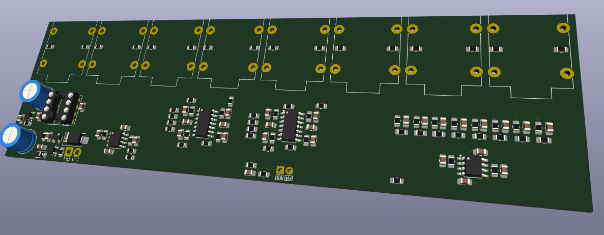
My good friend has a spaghetti cable routing dream that involves up to 8 loopers and so of course I’m spinning up a little design for them. It’ll have the ability to take 8 signals and mix them into 1, or take 1 signal and split it out to 8 different locations. Real simple buffers in both directions and resistor population options to pick the signal flow direction–I’m trying to keep it simple so there’s no user interface to control the flow. It’s gonna be a in a huge box.
Any time I make a guitar pedal enclosure design (which this buffer will be) I’ve gotten in the habit of throwing in my little crowbar over voltage and reverse voltage protection circuit. It’s nothing revolutionary (in fact I borrowed the idea from like 10 different reference designs) and it only really works at low current and fairly low voltages, but it’s enough to prevent bozos I sell stuff to from blowing things up.
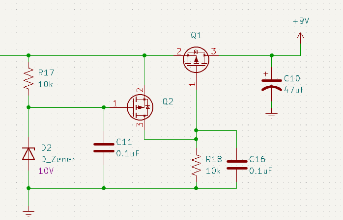
Anyway, it works like this. Under normal circumstances, i.e. when the system is powered by 9V nominal, Q1 is on and Q2 is off–both are P-channel MOSFETs. Q2 stays off because 9V doesn’t provide a high enough voltage to bias the zener diode D2 through R17 into clamping, so very little current flows through R17 holding the gate (pin 1) and the source (pin 2) of the FET close to each other and keeping Q2 shut off. With Q2 off, the gate of Q1 (pin 1) is held close to ground via R18. Meanwhile Q1’s source (pin 2) is equal to the input voltage, meaning we’ve got a gate to source voltage of 9V which is plenty to turn Q1 all the way on and power the system happily.
If a user plugs in something higher than about 10V, D2 will start to conduct more and more and regulate the voltage across itself to 10V, meaning as the input voltage rises, so too will the voltage across R17, thereby eventually turning on Q2 once the gate to source voltage gets sufficiently large. Once Q2 turns on, it shorts the gate and source of Q1, shutting it off, and protecting everything downstream from the overvoltage.
This whole circuit also gives us reverse polarity protection–if the input power polarity is flipped the gate of Q1 will forever be held above its source, keeping the power disconnected.
C11 and C16 are there to slow this whole process down just a little bit and to provide some low-rent ESD protection for the sensitive gates of my FETs.
This circuit isn’t perfect, but it does the job, and I get way fewer DMs about blown up electrolytics becuase of it.